LMX2346
LMX2346 is PLLatinum Frequency Synthesizer manufactured by National Semiconductor.
Description
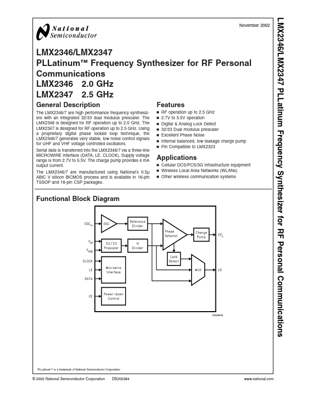
The LMX2346/7 are high performance frequency synthesizers with an integrated 32/33 dual modulus prescaler. The LMX2346 is designed for RF operation up to 2.0 GHz. The LMX2347 is designed for RF operation up to 2.5 GHz. Using a proprietary digital phase locked loop technique, the LMX2346/7 generates very stable, low noise control signals for UHF and VHF voltage controlled oscillators. Serial data is transferred into the LMX2346/7 via a three-line MICROWIRE interface (DATA, LE, CLOCK). Supply voltage range is from 2.7V to 5.5V. The charge pump provides 4 m A output current. The LMX2346/7 are manufactured using National’s 0.5µ ABi C V silicon Bi CMOS process and is available in 16-pin TSSOP and 16-pin CSP packages.
Features n n n n n n n RF operation up to 2.5 GHz 2.7V to 5.5V operation Digital & Analog Lock Detect 32/33 Dual modulus prescaler Excellent Phase Noise Internal balanced, low leakage charge pump Pin patible to LMX2323
Applications n Cellular DCS/PCS/3G infrastructure equipment n Wireless Local Area Networks (WLANs) n Other wireless munication systems
Functional Block Diagram
PLLatinum™ is a trademark of National Semiconductor Corporation.
© 2002 National Semiconductor Corporation
DS200384
.national.
LMX2346/LMX2347
Connection Diagrams
16-Pin TSSOP Package NS Package Number MTC16
16-Pin Chip Scale Package NS Package Number SLB16A
Pin Descriptions
Pin Number Pin Name OSCIN 16-Pin CSP 15 16-Pin I/O TSSOP 1 I Description
Reference oscillator input. A CMOS inverting gate input. The input has a VCC/2 input threshold and can be driven from an external CMOS or TTL logic gate. I/O Circuit Configuration
VP VCC
1 2
3 4
- Charge Pump Power Supply. Must be equal to VCC.
- Main Power Supply. VCC may range from 2.7V to 5.5V. Bypass capacitors should be placed as close as possible to this pin and be connected directly to the ground plane. O Charge Pump output. For connection to a loop filter for driving the voltage...