LMX9402
LMX9402 is Frequency Synthesizer Module manufactured by National Semiconductor.
Description
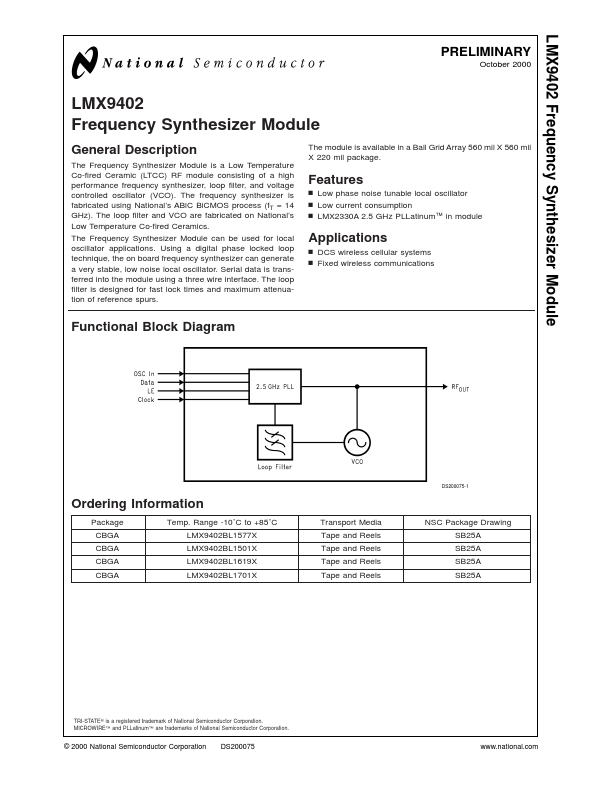
The Frequency Synthesizer Module is a Low Temperature Co-fired Ceramic (LTCC) RF module consisting of a high performance frequency synthesizer, loop filter, and voltage controlled oscillator (VCO). The frequency synthesizer is fabricated using National’s ABi C Bi CMOS process (f T = 14 GHz). The loop filter and VCO are fabricated on National’s Low Temperature Co-fired Ceramics. The Frequency Synthesizer Module can be used for local oscillator applications. Using a digital phase locked loop technique, the on board frequency synthesizer can generate a very stable, low noise local oscillator. Serial data is transferred into the module using a three wire interface. The loop filter is designed for fast lock times and maximum attenuation of reference spurs. The module is available in a Ball Grid Array 560 mil X 560 mil X 220 mil package.
Features n Low phase noise tunable local oscillator n Low current consumption n LMX2330A 2.5 GHz PLLatinum™ in module
Applications n DCS wireless cellular systems n Fixed wireless munications
Functional Block Diagram
DS200075-1
Ordering Information
Package CBGA CBGA CBGA CBGA Temp. Range -10˚C to +85˚C LMX9402BL1577X LMX9402BL1501X LMX9402BL1619X LMX9402BL1701X Transport Media Tape and Reels Tape and Reels Tape and Reels Tape and Reels NSC Package Drawing SB25A SB25A SB25A SB25A
TRI-STATE ® is a registered trademark of National Semiconductor Corporation. MICROWIRE™ and PLLatinum™ are trademarks of National Semiconductor Corporation.
© 2000 National Semiconductor Corporation
DS200075
.national.
Datasheet pdf
- http://..net/
.Data Sheet.co.kr
Connection Diagram
DS200075-2
Top View 25-Pin CBGA Package See NS Package Number SB25A
Pin Descriptions
Pin No. 1,2,3,4,5 6 7 8 9 10 11, 12 13 14, 15, 16 17 18, 19, 20 21 22 23 Pin Name GND LD GND VCC1 GND RFOUT GND VCC2 GND Data GND OSCIN CLK LE I/O
- O
- -
- O
- -
- I
- I I I Ground. Multiplexed output of the RF programmable dividers, reference dividers, or RF Lock...