LP3905
LP3905 is Power Management Unit For Low Power Handheld Applications manufactured by National Semiconductor.
Description
LP3905 is a multi-functional Power Management Unit, optimized for low power handheld applications. This device integrates two 600m A DC/DC buck regulators and two 150m A linear regulators. Fixed and adjustable buck output versions are available. The LP3905 additionally features two enable pins for the device output control and is offered in an LLP package.
Key Specifications
Buck Regulators n Fixed and adjustable voltage options, range 1.0V to 3.3V
- n Up to 90% Efficiency n Auto-switching PFM-PWM mode and fixed PWM mode n 2MHz PWM fixed switching frequency (Typ) n 600m A output current n ± 4% output voltage accuracy over temp. n Internal softstart n 2.2µH inductor, 10µF Input and 10µF output Caps Linear Regulators n Output options in the range 1.5V to 3.3V
- n 13.5µVrms output voltage noise n PSRR
- 70d B @ 1k Hz n ± 3% output voltage accuracy over full line and load regulation n 0m A to 150m A output current n Cin = 1.0µF, Cout = 0.47µF for 100m A O/P Cin = 1.0µF, Cout = 1.0µF for 150m A O/P 80m V Dropout voltage
- Fixed output voltage devices can be customized to fit system requirements. Please contact National Semiconductor Sales Office.
Features n Two buck regulators for powering high current processor functions or peripheral devices n Two linear regulators for powering internal processor functions and I/Os n One enable pin for Buck1 and Linear Regulators 1 & 2 n Separate enable pin for Buck2 n Thermal and current overload protection n Small 14- Pin LLP package (4mm x 4mm x 0.8mm)
Applications n n n n Baseband Processors Peripheral Processor (Video, Audio) I/O Power FPGA Power
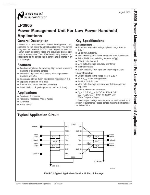
Typical Application Circuit
FIGURE 1. Typical Application Circuit
- 14 Pin LLP Package
© 2006 National Semiconductor Corporation
DS201529
.national.
Block Diagram
FIGURE 2. Simplified Functional Diagram
Connection Diagram
FIGURE 3. 14 Pin LLP Package
.national.
Connection Diagram Pin Descriptions
Pin # 1 2 3 4 5 6 7 8 9 10...