NV6252
Description
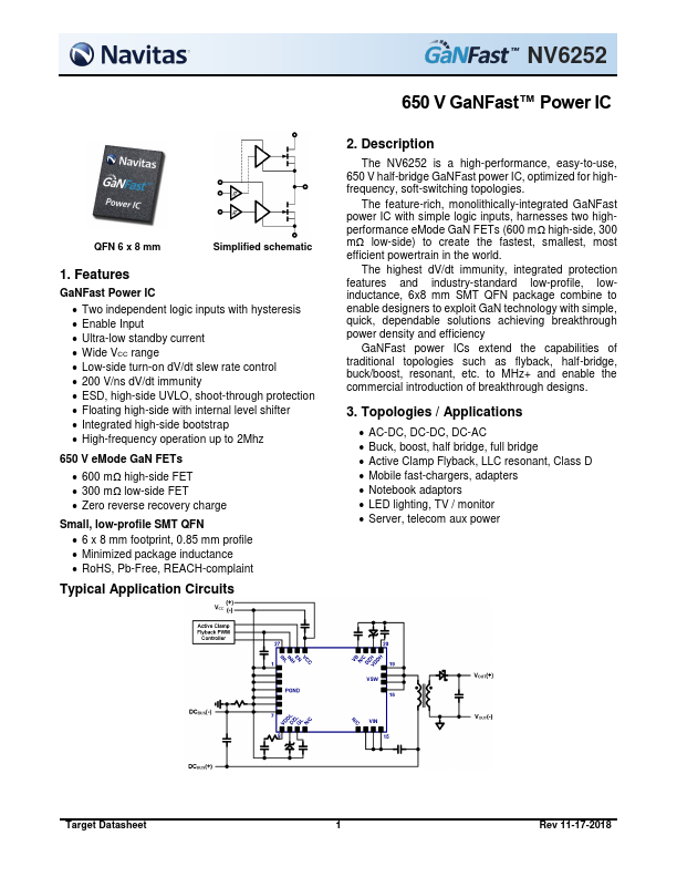
The NV6252 is a high-performance, easy-to-use, 650 V half-bridge GaNFast power IC, optimized for highfrequency, soft-switching topologies. The feature-rich, monolithically-integrated GaNFast power IC with simple logic inputs, harnesses two highperformance eMode GaN FETs (600 mΩ high-side, 300 mΩ low-side) to create the fastest, smallest, most efficient powertrain in the world.
Key Features
- Two independent logic inputs with hysteresis
- Enable Input
- Ultra-low standby current
- Wide VCC range
- Low-side turn-on dV/dt slew rate control
- 200 V/ns dV/dt immunity
- ESD, high-side UVLO, shoot-through protection
- Floating high-side with internal level shifter
- Integrated high-side bootstrap
- High-frequency operation up to 2Mhz 650 V eMode GaN FETs