DESCRIPTION
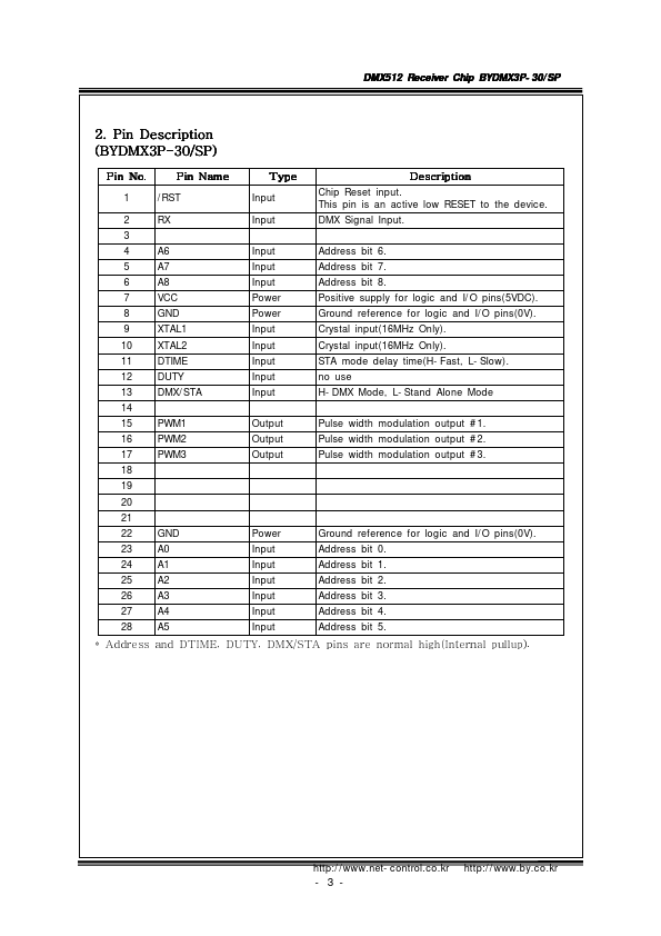
(BYDMX3P-30/SP) Pin No. 1 2 3 4 5 6 7 8 9 10 11 12 13 14 15 16 17 18 19 20 21 22 23 24 25 26 27 28 A6 A7 A8 RX Pin Name / RST Type Input Input Input Input Input Power Power Input Input Input Input Input Output Output Output DMX Signal Input. Address bit 6. Address bit 7. Address bit 8. DESCRIPTION
Chip Reset input. This pin is an active low RESET to the device. VCC GND XTAL1 XTAL2 DTIME DUTY DMX/ STA PWM1 PWM2 PWM3 Positive supply for logic and I/ O pins(5VDC). Ground reference for logic and I/ O pins(0V). Crystal input(16MHz Only). Crystal input(16MHz Only). STA mode delay time(H- Fast, L- Slow). no use H- DMX Mode, L- Stand Alone Mode Pulse width modulation output # 1. Pulse width modulation output # 2. Pulse width modulation output # 3. GND A0 A1 A2 A3 A4 A5 Power Input Input Input Input Input Input Ground reference for logic and I/ O pins(0V). Address bit 0. Address bit 1. Address bit 2. Address bit 3. Address bit 4. Address bit 5. * Address and DTIME, DUTY, DMX/STA pins are normal high(Internal pullup). http:/ / control.co.kr http:/ / - 3 - DMX512 Receiver Chip BYDMX3P- 30/ SP (BYDMX3P-31/TQFP) Pin No.