GENERAL DESCRIPTION
Two stage amplifier and ESD protection circuit are integrated in the IC to achieve very high gain and high ESD tolerance. An ultra-small and ultra-thin package of FLP6-A1 is adopted. ! FEATURES
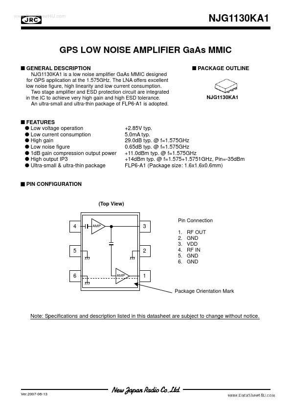
" Low voltage operation " Low current consumption " High gain " Low noise figure " 1dB gain compression output power " High output IP3 " Ultra-small & ultra-thin package ! PIN CONFIGURATION ! PACKAGE OUTLINE NJG1130KA1 +2.85V typ. 5.0mA typ. 29.0dB typ. @ f=1.575GHz 0.65dB typ. @ f=1.575GHz +11.0dBm typ. @ f=1.575GHz +14dBm typ. @ f=1.575+1.5751GHz, Pin=-35dBm FLP6-A1 (Package size: 1.6x1.6x0.6mm) (Top View) Pin Connection 4 AMP 3 1. 2. 3. 4. 5. 6. RF OUT GND VDD RF IN GND GND 5 2 6 AMP 1 Package Orientation Mark Note: Specifications and description listed in this datasheet are subject to change without notice. Ver.2007-06-13 -1- NJG1130KA1 ! ABSOLUTE MAXIMUM RATINGS
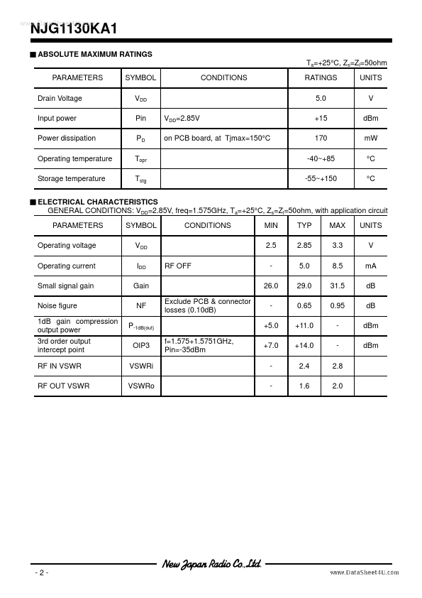
Ta=+25°C, Zs=Zl=50ohm PARAMETERS Drain Voltage Input power Power dissipation Operating temperature Storage temperature SYMBOL VDD Pin PD Topr Tstg VDD=2.85V on PCB board, at Tjmax=150°C CONDITIONS RATINGS 5.0 +15 170 -40~+85 -55~+150 UNITS V dBm mW °C °C ! New Japan Radio