GENERAL DESCRIPTION
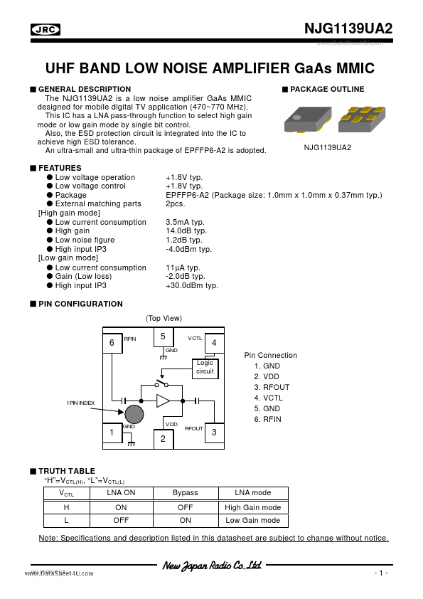
Also, the ESD protection circuit is integrated into the IC to achieve high ESD tolerance. An ultra-small and ultra-thin package of EPFFP6-A2 is adopted. ! PACKAGE OUTLINE NJG1139UA2 ! FEATURES
" Low voltage operation " Low voltage control " Package " External matching parts [High gain mode] " Low current consumption " High gain " Low noise figure " High input IP3 [Low gain mode] " Low current consumption " Gain (Low loss) " High input IP3 ! PIN CONFIGURATION +1.8V typ. +1.8V typ. EPFFP6-A2 (Package size: 1.0mm x 1.0mm x 0.37mm typ.) 2pcs. 3.5mA typ. 14.0dB typ. 1.2dB typ. -4.0dBm typ. 11 µA typ. -2.0dB typ. +30.0dBm typ. (Top View) 6 RFIN 5 GND VCTL 4 Pin Connection 1. GND 2. VDD 3. RFOUT 4. VCTL 5. GND 6. RFIN Logic circuit 1PIN INDEX 1 GND VDD RFOUT 2 3 ! TRUTH TABLE “H”=VCTL(H), “L”=VCTL(L) VCTL H L LNA ON ON OFF Bypass OFF ON LNA mode High Gain mode Low Gain mode Note: Specifications and description listed in this datasheet are subject to change without notice. Ver.2009-9-18 -1- NJG1139UA2 ! New Japan Radio