New Japan Radio NJG1142KA1
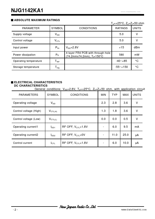
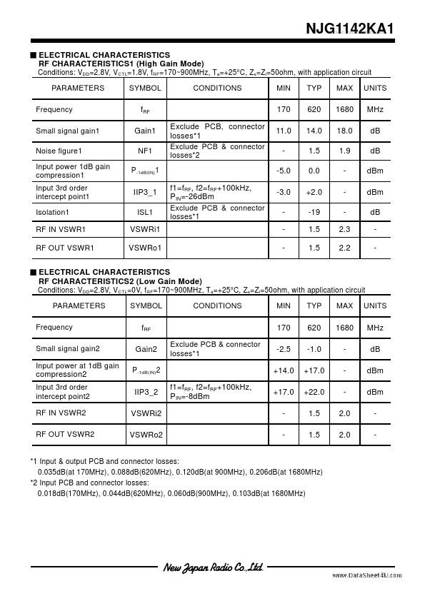
The NJG1142KA1 is a wide band low noise amplifier GaAs MMIC designed for mobile TV application. The NJG1142KA1 has a LNA pass-through function to select high gain mode or low gain mode by low control voltage operation. The NJG1142KA1 features low current consumption, high linearity.| Part No. | NJG1142KA1 |
|---|---|
| Datasheet | NJG1142KA1 Download |
| Manufacturer |  New Japan Radio |
| Description | WIDE BAND LOW NOISE AMPLIFIER GaAs MMIC |
| Buy | Stock & Price |

GENERAL DESCRIPTION
And this amplifier can be tuned to wide frequency (170~1680MHz). An ultra-small and ultra-thin package of FLP6-A1 is adopted.FEATURES
Wide operating frequency range 170MHz~1680MHz Low voltage operation 2.8V typ. [High gain mode] Low current consumption 6mA typ. High gain +14.0dB typ. Low noise figure 1.5dB typ. High P-0.1dB Compression 0dBm typ. High input IP3 +2.0dBm typ. [Low gain mode] Low current consumption 11 μA typ. Gain (Low loss) -1.0dB typ. High P-0.1dB Compression +17dBm typ. High input IP3 +22.0dBm typ. External components count Small package size Lead -free and halogen-free PIN CONFIGURATION (Top View) PIN CONNECTION 1. VCTL 2. GND 3. RFOUT 4. GND 5. GND 6. RFIN TRUTH TABLE 6 RFIN PACKAGE OUTLINE NJG1142KA1 3 pcs. (capacitor: 2pcs, inductor: 1pc) FLP6-A1 (package size: 1.6mm x 1.6mm x 0.55mm typ.) 4 GND 3 RFOUT 5 GND Bias circuit 2 GND Logic circuit 1 VCTL “H” = VCTL(H) “L” = VCTL(L) VCTL H L LNA Mode High Gain Mode Low Gain Mode 1Pin INDEX NOTE: The i...