DESCRIPTION
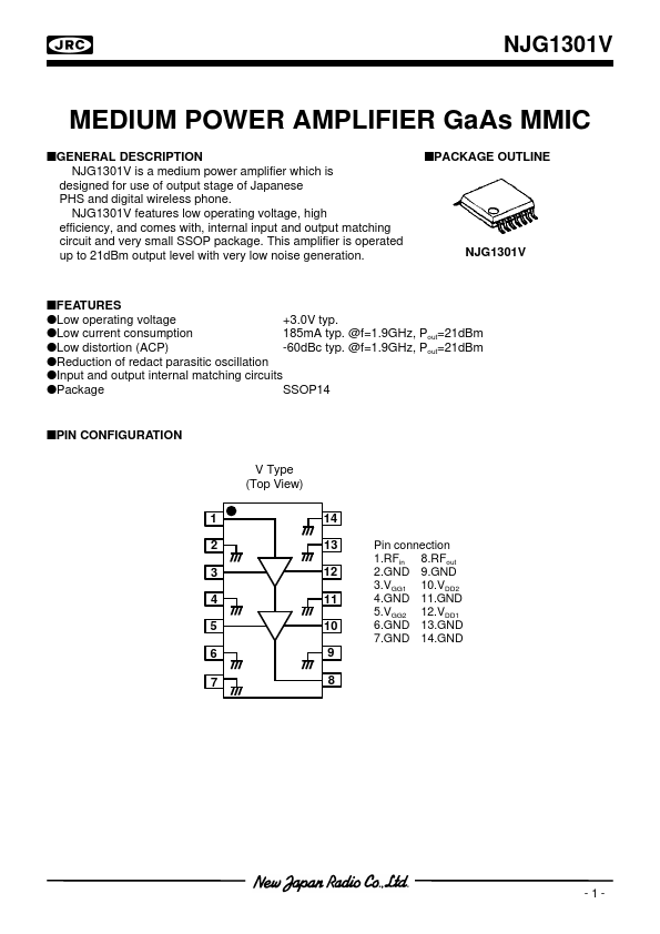
NJG1301V features low operating voltage, high efficiency, and comes with, internal input and output matching circuit and very small SSOP package. nPACKAGE OUTLINE NJG1301V nFEATURES lLow operating voltage +3.0V typ. lLow current consumption 185mA typ. @f=1.9GHz, Pout=21dBm lLow distortion (ACP) -60dBc typ. @f=1.9GHz, Pout=21dBm lReduction of redact parasitic oscillation lInput and output internal matching circuits lPackage SSOP14 nPIN CONFIGURATION V Type (Top View) 1 2 3 4 5 6 7 14 13 12 11 10 9 8 Pin connection 1.RFin 8.RFout 2.GND 9.GND 3.VGG1 10.VDD2 4.GND 11.GND 5.VGG2 12.VDD1 6.GND 13.GND 7.GND 14.GND -1- NJG1301V nABSOLUTE MAXIMUM RATINGS
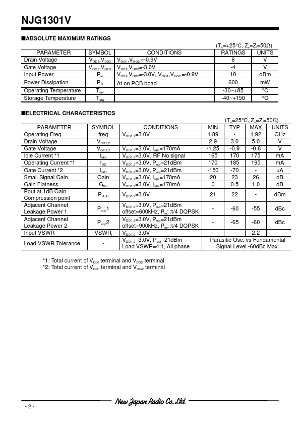
PARAMETER Drain Voltage Gate Voltage Input Power Power Dissipation Operating Temperature Storage Temperature SYMBOL VDD1,VDD2 VGG1,VGG2 Pin PD Topr Tstg CONDITIONS VGG1,VGG2 =-0.9V VDD1,VDD2=-3.0V VDD1,VDD2=-3.0V, VGG1,VGG2 =-0.9V At on PCB boad (Ta=+25°C, Zs=Zl=50Ω) RATINGS UNITS 6 V -4 V 10 dBm 600 mW -30~+85 °C -40~+150 °C nELECTRICAL CHARACTERISTICS PARAMETER Operating Freq. New Japan Radio