Datasheet4U Logo Datasheet4U.com

NJG1650HB6 - SP3T SWITCH GaAs MMIC

General Description

NJG1650HB6 is a SP3T switch IC featured low insertion loss, high isolation and small size package.

This switch is suitable for W-LAN, Bluetooth, and sub-microwave applications.

A small and thin package of USB8-B6 is adopted.

Key Features

  • G Control voltage range G Low insertion loss G High isolation G Input power at 0.2dB compression point G Low current consumption G Small & thin package +2.0~+5.0V 0.38dB typ. @f=1.0GHz, PIN=23dBm, VCTL(H)=2.7V 0.42dB typ. @f=2.0GHz, PIN=23dBm, VCTL(H)=2.7V 0.45dB typ. @f=2.5GHz. PIN=23dBm, VCTL(H)=2.7V 21dB typ. @f=2.5GHz, PIN=23dBm, VCTL(H)=2.7V 28dBm typ. @f=2.5GHz, VCTL(H)=2.7V 5µA typ. @ VCTL(H)=2.7V USB8-B6 (package Size: 1.5 x 1.5 x 0.55mm typ. ) I PIN.

📥 Download Datasheet

Full PDF Text Transcription (Reference)

The following content is an automatically extracted verbatim text from the original manufacturer datasheet and is provided for reference purposes only.

View original datasheet text
NJG1650HB6 SP3T SWITCH GaAs MMIC I GENERAL DESCRIPTION NJG1650HB6 is a SP3T switch IC featured low insertion loss, high isolation and small size package. This switch is suitable for W-LAN, Bluetooth, and sub-microwave applications. A small and thin package of USB8-B6 is adopted. I APPLICATIONS LTE and 3G applications WLAN and Blue-tooth applications Receive system, RX path, and Diversity antenna applications Mobile phone, Tablet PC, Data card, Modem and Router applications 
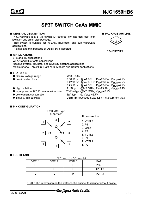
I PACKAGE OUTLINE NJG1650HB6 I FEATURES G Control voltage range G Low insertion loss G High isolation G Input power at 0.2dB compression point G Low current consumption G Small & thin package +2.0~+5.0V 0.38dB typ. @f=1.0GHz, PIN=23dBm, VCTL(H)=2.7V 0.42dB typ. @f=2.0GHz, PIN=23dBm, VCTL(H)=2.7V 0.45dB typ. @f=2.