Datasheet4U Logo Datasheet4U.com

NJM8513 - JFET Input Operational Amplifier

Download the NJM8513 datasheet PDF. This datasheet also covers the NJM8512 variant, as both devices belong to the same jfet input operational amplifier family and are provided as variant models within a single manufacturer datasheet.

General Description

The NJM8512/NJM8513 are Dual/Quad high p

Key Features

  • Low Input Offset Voltage VIO=400μV max. VIO=700μV max. (Ta= -40°C to +125°C).
  • Low Input Offset Voltage Drift ΔVIO/ΔT=5μV/°C max. (Ta= -40°C to +125°C).
  • Low Supply Current Icc=1.3mA /ch typ.
  • High Slew Rate SR=20V/μs typ.
  • Wide Bandwidth ft=7MHz typ.
  • Low Noise en=10nV/Hz typ. (at f=1kHz ).
  • Low Input Bias Current.
  • No Phase Reversal IB=80pA max. (at Ta=25°C).
  • RF noise Immunity.
  • Guaranteed Temperature Topr= -40°C to +125°C.
  • Operating.

📥 Download Datasheet

Note: The manufacturer provides a single datasheet file (NJM8512-NewJapanRadio.pdf) that lists specifications for multiple related part numbers.

Full PDF Text Transcription (Reference)

The following content is an automatically extracted verbatim text from the original manufacturer datasheet and is provided for reference purposes only.

View original datasheet text
NJM8512/NJM8513 Precision, JFET Input Operational Amplifier 
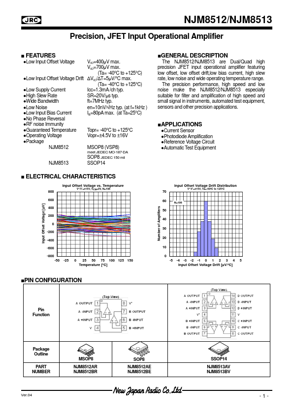
Input Offset Voltage [μV] Number of Amplifiers ■ FEATURES ●Low Input Offset Voltage VIO=400μV max. VIO=700μV max. (Ta= -40°C to +125°C) ●Low Input Offset Voltage Drift ΔVIO/ΔT=5μV/°C max. (Ta= -40°C to +125°C) ●Low Supply Current Icc=1.3mA /ch typ. ●High Slew Rate SR=20V/μs typ. ●Wide Bandwidth ft=7MHz typ. ●Low Noise en=10nV/Hz typ. (at f=1kHz ) ●Low Input Bias Current ●No Phase Reversal IB=80pA max. (at Ta=25°C) ●RF noise Immunity ●Guaranteed Temperature Topr= -40°C to +125°C ●Operating Voltage Vopr=±4.5V to ±16V ●Package NJM8512 MSOP8 (VSP8) meet JEDEC MO-187-DA SOP8 JEDEC 150 mil NJM8513 SSOP14 ■ ELECTRICAL CHARACTERISTICS Input Offset Voltage vs.