DESCRIPTION
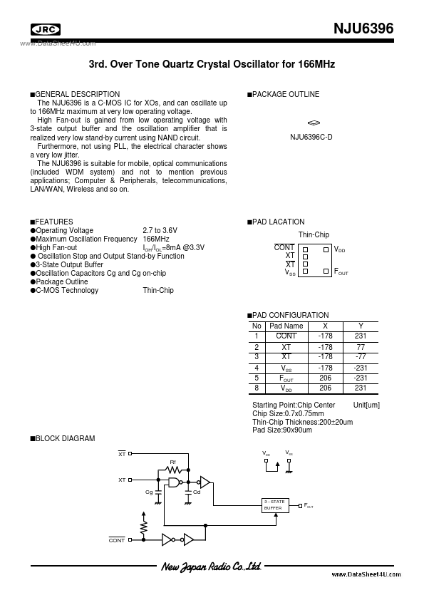
sPACKAGE OUTLINE High Fan-out is gained from low operating voltage with 3-state output buffer and the oscillation amplifier that is realized very low stand-by current using NAND circuit. Furthermore, not using PLL, the electrical character shows a very low jitter. NJU6396C-D sFEATURES qOperating Voltage 2.7 to 3.6V qMaximum Oscillation Frequency 166MHz qHigh Fan-out IOH/IOL=8mA @3.3V q Oscillation Stop and Output Stand-by Function q3-State Output Buffer qOscillation Capacitors Cg and Cg on-chip qPackage Outline qC-MOS Technology Thin-Chip sPAD LACATION Thin-Chip CONT XT XT VSS VDD FOUT sPAD CONFIGURATION No 1 2 3 4 5 8 Pad Name CONT XT XT VSS FOUT VDD X -178 -178 -178 -178 206 206 Y 231 77 -77 -231 -231 231 Starting Point:Chip Center Unit[um] Chip Size:0.7x0.75mm Thin-Chip Thickness:200±20um Pad Size:90x90um sBLOCK DIAGRAM XT VDD VSS Rf XT Cg Cd 3 − STATE BUFFER FOUT CONT 2003/03/07 ( 1 / 4 ) NJU6396 sTREMINAL DESCRIPTION
SYMBOL FUNCTION Oscillation and 3-state Output Buffe... New Japan Radio