NJW4190 Overview
Key Specifications
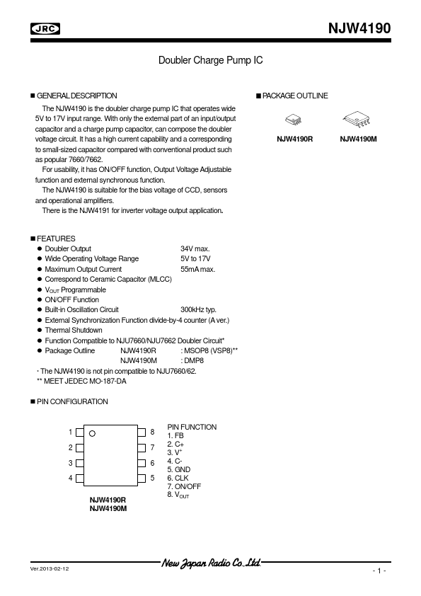
Package: TSSOP
Max Operating Temp: 85 °C
Min Operating Temp: -40 °C
Description
The NJW4190 is the doubler charge pump IC that operates wide 5V to 17V input range. With only the external part of an input/output capacitor and a charge pump capacitor, can compose the doubler voltage circuit.
Key Features
- Doubler Output 34V max
- Wide Operating Voltage Range 5V to 17V Maximum Output Current 55mA max
- Correspond to Ceramic Capacitor (MLCC) VOUT Programmable ON/OFF Function Built-in Oscillation Circuit 300kHz typ
- ** MEET JEDEC MO-187-DA