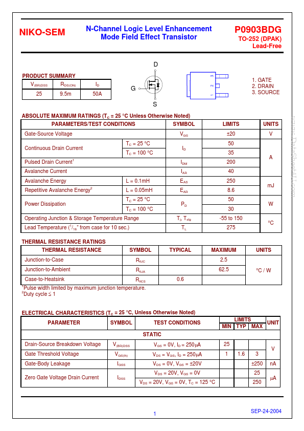
| Part | 903BDG |
|---|---|
| Description | P0903BDG |
| Manufacturer | Niko-Sem |
| Size | 303.87 KB |
Pricing from 0.1523 USD, available from UnikeyIC and Unikeyic (ICkey).
Price & Availability
| Seller | Inventory | Price Breaks | Buy |
|---|---|---|---|
| UnikeyIC | 400000 | 100+ : 0.1523 USD 200+ : 0.1498 USD 300+ : 0.1459 USD |
View Offer |
| Unikeyic (ICkey) | 400000 | 100+ : 0.1523 USD 200+ : 0.1498 USD 300+ : 0.1459 USD |
View Offer |
Related Datasheets
| Part Number | Manufacturer | Description |
|---|---|---|
| 903133-xx | Accurate Screw Machine | Lock Washers |
| 903149-xx | Accurate Screw Machine | Lock Washers |
| 903184-xx | Accurate Screw Machine | Lock Washers |
| 903185-xx | Accurate Screw Machine | Lock Washers |
| 903186-xx | Accurate Screw Machine | Lock Washers |

