Niko-Sem P70N02LS
N-Channel Logic Level Enhancement Mode Field Effect Transistor
| Part No. | P70N02LS |
|---|---|
| Datasheet | P70N02LS Download |
| Manufacturer |  Niko-Sem |
| Description | N-Channel Logic Level Enhancement Mode Field Effect Transistor |
| Buy | Stock & Price |

ABSOLUTE MAXIMUM RATINGS
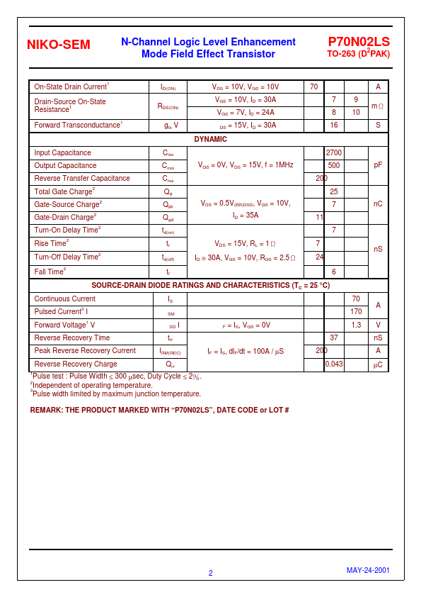
(TC = 25 °C Unless Otherwise Noted) PARAMETERS/TEST CONDITIONS Gate-Source Voltage Continuous Drain Current Pulsed Drain Current Avalanche Current Avalanche Energy Repetitive Avalanche Energy Power Dissipation 2 1 SYMBOL VGS ± LIMITS 20 70 45 170 60 140 5.6 65 38 -55 to 150 UNITS V TC = 25 °C TC = 100 °C ID IDM IAR A L = 0.1mH L = 0.05mH TC = 25 °C TC = 100 °C EAS EAR PD Tj, Tstg TL 275 mJ W Operating Junction & Storage Temperature Range Lead Temperature ( /16” from case for 10 sec.) THERMAL RESISTANCE RATINGS THERMAL RESISTANCE Junction-to-Case Junction-to-Ambient Case-to-Heatsink 1 2 1 °C SYMBOL RθJC RθJA RθCS TYPICAL MAXIMUM 2.3 62.5 UNITS °C / W 0.6 Pulse width limited by maximum junction temperature. Duty cycle ≤ 1%ELECTRICAL CHARACTERISTICS
(TC = 25 °C, Unless Otherwise Noted) PARAMETER SY MBOL TEST CONDITIONS STATIC Drain-Source Breakdown Voltage Gate Threshold Voltage Gate-Body Leakage Zero Gate Voltage Drain Current V(BR)DSS VGS(th) IGSS V IDSS VGS =...