The following content is an automatically extracted verbatim text
from the original manufacturer datasheet and is provided for reference purposes only.
View original datasheet text
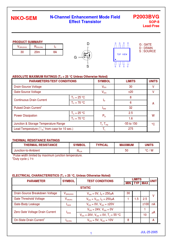
NIKO-SEM
N-Channel Enhancement Mode Field Effect Transistor
P2003BVG
SOP-8 Lead-Free
PRODUCT SUMMARY
V(BR)DSS
RDS(ON)
30 20m
ID 8A
D
G S
ABSOLUTE MAXIMUM RATINGS (TC = 25 °C Unless Otherwise Noted)
PARAMETERS/TEST CONDITIONS
SYMBOL
Drain-Source Voltage
Gate-Source Voltage
Continuous Drain Current Pulsed Drain Current1
TC = 25 °C TC = 70 °C
Power Dissipation
TC = 25 °C TC = 70 °C
Junction & Storage Temperature Range Lead Temperature (1/16” from case for 10 sec.)
VDS VGS
ID
IDM
PD
Tj, Tstg TL
THERMAL RESISTANCE RATINGS THERMAL RESISTANCE
SYMBOL
Junction-to-Ambient
RθJA
1Pulse width limited by maximum junction temperature.
2Duty cycle ≤ 1%
TYPICAL
G : GATE D : DRAIN S : SOURCE
LIMITS 30 ±20 8 6 32 2.5 1.