N- & P-Channel Enhancement Mode Field Effect Transistor
Full PDF Text Transcription (Reference)
The following content is an automatically extracted verbatim text
from the original manufacturer datasheet and is provided for reference purposes only.
View original datasheet text
NIKO-SEM
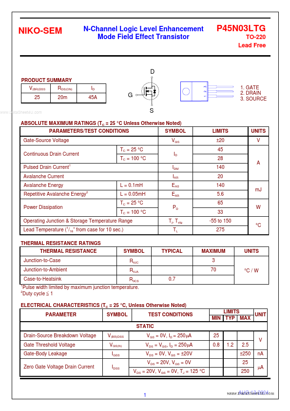
N-Channel Logic Level Enhancement Mode Field Effect Transistor
P45N03LTG
TO-220 Lead Free
D
PRODUCT SUMMARY V(BR)DSS 25
www.DataSheet4U.com
RDS(ON) 20m
ID 45A
G S
1. GATE 2. DRAIN 3. SOURCE
ABSOLUTE MAXIMUM RATINGS (TC = 25 °C Unless Otherwise Noted) PARAMETERS/TEST CONDITIONS Gate-Source Voltage Continuous Drain Current Pulsed Drain Current Avalanche Current Avalanche Energy Repetitive Avalanche Energy2 Power Dissipation L = 0.1mH L = 0.05mH TC = 25 °C TC = 100 °C Operating Junction & Storage Temperature Range Lead Temperature ( /16” from case for 10 sec.) THERMAL RESISTANCE RATINGS THERMAL RESISTANCE Junction-to-Case Junction-to-Ambient Case-to-Heatsink
1 2 1 1
SYMBOL VGS
LIMITS ±20 45 28 140 20 140 5.