CF5741BB
CF5741BB is Analog Clock CMOS IC manufactured by Nippon Precision Circuits Inc.
OVERVIEW
The CF5741 series are analog clock driver ICs using 32.768k Hz reference frequency of crystal oscillator. Some versions in accordance with the binations of each motor drive and alarm output characteristics can provide a wide range of applications for various clock specifications.
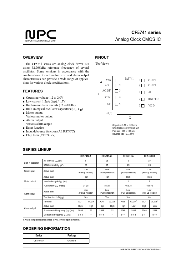
PINOUT
(Top View)
VSS AO1 AO2/F Y XTN XT (0,0)
1 2 3 4 5
SA5741
10 9 8 7 6
OUT2 OUT1 AI RST/TC VDD
FEATURES s s s s s s s s s
Operating voltage 1.2 to 2.0V Low current 1.2µA (typ) / 1.5V Built-in oscillator circuits (32.768 k Hz) Built-in crystal oscillator capacitors (CG, CD) Motor output Various motor output Alarm output Various alarm output Reset function Input debounce function (AI, RST/TC) Chip form (CF5741××)
Chip size : 1.22 × 1.20 mm Chip thickness : 400 ± 30 µm Pad size : 100 × 100 µm Reverse side : V DD level
SERIES LINEUP
CF5741AA Built-in capacitor Reset input XT terminal CG (p F) XTN terminal CD (p F) Active level Active level Motor output Hand drive cycle t CY (sec) Pulse width t PW (msec) Alarm input Active level Test function (1/2VDD ) Terminal Alarm output Active level Fundamental frequency f PW (Hz) Modulation frequency f CY (Hz) AO1 High 2048 8+1 0 25 Low (Pull-up resistor) High 1 31.25 Low (Pull-up resistor) Yes AO2/F High 32
- AO1 High 2048 8+1 CF5741AB 25 25 Low (Pull-up resistor) High 1 31.25 Low (Pull-up resistor) Yes AO2/F High 32
- AO1 High 2048 8+1 CF5741BA 0 25 Low (Pull-up resistor) High 1 46.875 Low (Pull-up resistor) Yes AO2/F1 Low 2048 8+1 AO1 High 2048 8+1 CF5741BB 27 25 Low (Pull-up resistor) High 1 46.875 Low (Pull-up resistor) Yes AO2/F1 Low 2048 8+1
1. AO is plete reverse phase of AO. (even output is inactive.)
ORDERING INFORMATION
Device CF5741×× Package Chip form
NIPPON PRECISION CIRCUITS- 1
CF5741 series
BLOCK DIAGRAM
4 Stage Divider
13 Stage Divider
XTN RST/TC Reset Input
Alarm Input
Alarm Test
AO Test
Alarm Output Control
Motor Output Control
AO1 AO2/F
OUT1 OUT2
PIN...