SM8761 Overview
Key Features
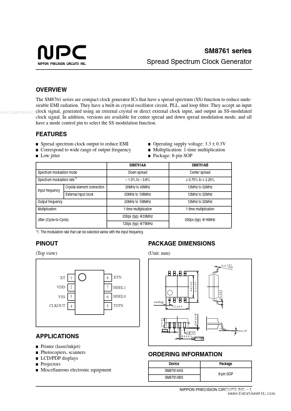
- The modulation rate that can be selected varies with the input frequency
| Part | SM8761 |
|---|---|
| Description | Spread Spectrum Clock Generator |
| Manufacturer | Nippon Precision Circuits |
| Size | 163.39 KB |
| Part Number | Manufacturer | Description |
|---|---|---|
| XR2206 | Exar | Monolithic Function Generator |
| AN97 | Maxim Integrated | Telephone Tone Generator |
| AN97 | Maxim Integrated | Telephone Tone Generator Requires No trimming |