NC1M120C75HTU
Features
- High blocking voltage with low On-resistance
- High speed switching with low capacitances
- Fast intrinsic diode with low reverse recovery (Qrr)
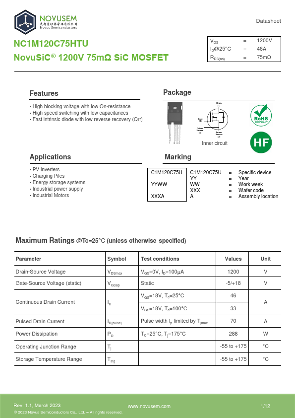
Package
Drain (1)
1 2 34
Gate (4)
Driver Source
(3)
Power Source
(2)
Inner circuit
Applications
Marking
- PV Inverters
- Charging Piles
- Energy storage systems
- Industrial power supply
- Industrial Motors
C1M120C75U C1M120C75U = Specific device
= Year
YYWW
= Work week
= Wafer code
XXXA
= Assembly location
Maximum Ratings @Tc=25°C (unless otherwise specified)
Parameter Drain-Source Voltage Gate-Source Voltage (static)
Continuous Drain Current
Pulsed Drain Current Power Dissipation Operating Junction Range Storage Temperature Range
Symbol VDSmax VGSop
ID(pulse) PD Tj Tstg
Test conditions VGS=0V, ID=100μA Static VGS=18V, Tc=25°C VGS=18V, Tc=100°C Pulse width tp limited by Tjmax TC=25°C, Tj=175°C
Values 1200...