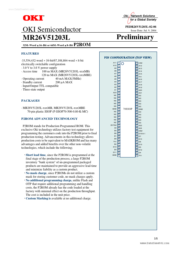
Datasheet4U Logo Datasheet4U.com

MR26V51203L - 32M-Word x 16-Bit or 64M-Word x 8-Bit

Datasheet Summary

Description

Pin name D15 / A 1 A0 to A24 D0 to D14 CE# OE# BYTE# VCC VSS Address inputs Data outputs Chip enable input Output enable input Word / Byte select input Power supply voltage Ground Functions Data output / Address input 2/8 www.DataSheet4U.com PEDR26V51203L-02-06 OKI Semiconductor MR26V5

Features

  • 33,554,432-word × 16-bit/67,108,864-word × 8-bit electrically switchable configuration.
  • 3.0 V to 3.6 V power supply.
  • Access time 100 ns MAX (MR26V51203L-xxxMB) 120 ns MAX (MR26V51203L-xxxMBE).
  • Operating current 40 mA MAX(5MHz).
  • Standby current 200 µA MAX.
  • Input/Output TTL compatible.
  • Three-state output CE# A12 A13 A14 A15 Vcc A16 A17 A18 A19 A20 A21 NC NC NC NC NC GND NC NC NC NC NC A22 A24 OE# D15/A-1 D7 D14 D6 D13 D5 D12 D4 Vcc.

📥 Download Datasheet

Datasheet preview – MR26V51203L

Datasheet Details

Part number MR26V51203L
Manufacturer OKI electronic componets
File Size 122.66 KB
Description 32M-Word x 16-Bit or 64M-Word x 8-Bit
Datasheet download datasheet MR26V51203L Datasheet
Additional preview pages of the MR26V51203L datasheet.
Other Datasheets by OKI electronic componets

Full PDF Text Transcription

Click to expand full text
www.DataSheet4U.com OKI Semiconductor MR26V51203L 32M–Word × 16–Bit or 64M–Word × 8–Bit PEDR26V51203L-02-06 Issue Date: Jul. 9, 2004 Preliminary PIN CONFIGURATION (TOP VIEW) A11 A10 A9 A8 A7 A6 A5 A4 A3 A2 A1 A23 NC NC NC NC NC GND NC NC NC NC NC BYTE# A0 D0 D8 D1 D9 Vcc D2 D10 D3 D11 GND 1 2 3 4 5 6 7 8 9 10 11 12 13 14 15 16 17 18 19 20 21 22 23 24 25 26 27 28 29 30 31 32 33 34 35 70 69 68 67 66 65 64 63 62 61 60 59 58 57 56 55 54 P2ROM FEATURES ·33,554,432-word × 16-bit/67,108,864-word × 8-bit electrically switchable configuration · 3.0 V to 3.
Published: |