04N50Z
Features
- -
- -
Low ON Resistance Low Gate Charge 100% Avalanche Tested These Devices are Pb- Free and are Ro HS pliant
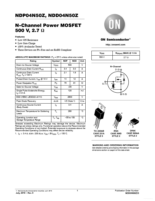
VDSS 500 V http://onsemi.
RDS(on) (MAX) @ 1.5 A 2.7 W
ABSOLUTE MAXIMUM RATINGS (TC = 25°C unless otherwise noted)
Rating Drain- to- Source Voltage Continuous Drain Current Rq JC Continuous Drain Current Rq JC, TA = 100°C Pulsed Drain Current, VGS @ 10 V Power Dissipation Rq JC Gate- to- Source Voltage Single Pulse Avalanche Energy, ID = 3.4 A ESD (HBM) (JESD22- A114) Peak Diode Recovery Continuous Source Current (Body Diode) Maximum Temperature for Soldering Leads Operating Junction and Storage Temperature Range Symbol VDSS ID ID IDM PD VGS EAS Vesd dv/dt IS TL TJ, Tstg 3.4 2.1 14 75 ±30 120 2800 4.5 (Note 1) 3.4 260
- 55 to 150 NDP 500 3.0 1.9 12 61 NDD Unit V A A A W V m J
N- Channel D (2)
G (1)
S (3) V V/ns A °C °C 1 2
4 4 1 1
Stresses exceeding Maximum Ratings may damage the device. Maximum Ratings are stress ratings only. Functional operation above the Remended...