2SK932
Features
- Adoption of FBET Process
- Large | yfs |
- Small Ciss
- Ultralow Noise Figure
- Ultrasmall- sized Package Permitting 2SK932- applied Sets to be
Made Smaller and Slimer
- These are Pb- Free Devices
Specifications
ABSOLUTE MAXIMUM RATINGS ( TA = 25°C)
Parameter
Symbol Conditions Ratings Unit
Drain- to- Source Voltage Gate- to- Drain Voltage Gate Current Drain Current Allowable Power Dissipation Junction Temperature
VDSX VGDS
IG ID PD Tj
- 15
10 m A
50 m A
200 m W
°C
Storage Temperature
Tstg
- 55 to +150 °C
Stresses exceeding those listed in the Maximum Ratings table may damage the device. If any of these limits are exceeded, device functionality should not be assumed, damage may occur and reliability may be affected.
DATA SHEET .onsemi.
1 2
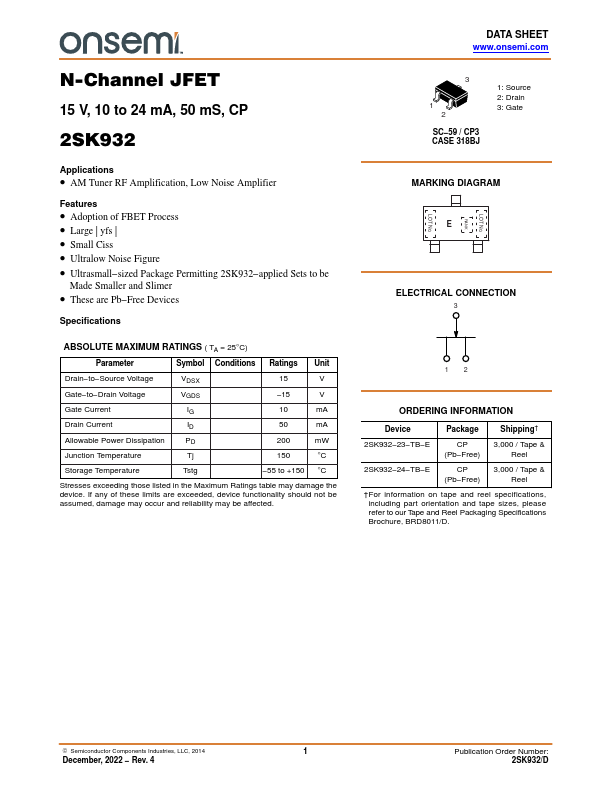
SC- 59 / CP3 CASE 318BJ
1: Source 2: Drain 3: Gate
MARKING DIAGRAM
LOT No.
RANK
LOT No.
ELECTRICAL...