74AC273
74AC273 is Octal D Flip-Flop manufactured by onsemi.
Features http://onsemi.
20 1
PDIP- 20 SUFFIX N CASE 738
- -
- -
- -
- -
- -
Ideal Buffer for MOS Microprocessor or Memory Eight Edge-Triggered D Flip- Flops Buffered mon Clock Buffered, Asynchronous Master Reset See MC74AC377 for Clock Enable Version See MC74AC373 for Transparent Latch Version See MC74AC374 for 3-State Version Outputs Source/Sink 24 m A ′ACT273 Has TTL patible Inputs Pb- Free Packages are Available-
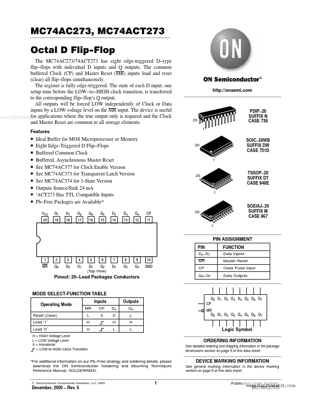
VCC 20 Q7 19 D7 18 D6 17 Q6 16 Q5 15 D5 14 D4 13 Q4 12 CP 11
SOIC- 20WB SUFFIX DW CASE 751D 1 TSSOP- 20 SUFFIX DT CASE 948E 1 SOEIAJ- 20 SUFFIX M CASE 967 1
PIN ASSIGNMENT
PIN D0- D7 1 MR 2 Q0 3 D0 4 D1 5 6 7 D2 8 D3 9 Q3 10 GND MR CP Q0- Q7 Q1 Q2 (Top View) FUNCTION Data Inputs Master Reset Clock Pulse Input Data Outputs
Pinout: 20- Lead Packages Conductors
MODE SELECT-FUNCTION TABLE
Operating Mode Reset (Clear) Load ′1′ Load ′0′ Inputs MR L H H CP X Dn X H L Outputs Qn L H L
D0 D1 D2 D3 D4 D5 D6 D7 CP MR Q0 Q1 Q2 Q3 Q4 Q5 Q6 Q7
Logic Symbol ORDERING INFORMATION
See detailed ordering and shipping information in the package dimensions section on page 5 of this data sheet.
H = HIGH Voltage Level L = LOW Voltage Level X = Immaterial = LOW-to-HIGH Clock Transition
- For additional information on our Pb- Free strategy and soldering details, please download the ON Semiconductor Soldering and Mounting Techniques Reference Manual, SOLDERRM/D.
© Semiconductor ponents Industries, LLC, 2005
DEVICE MARKING INFORMATION
See general marking information in the device marking section on page 6 of this data sheet.
December, 2005
- Rev. 6
Publication Order Number: MC74AC273/D
MC74AC273, MC74ACT273
D0 CP D1 D2 D3 D4 D5 D6 D7
Q CP RD
Q CP RD
Q CP...