74VHC1GT08 Overview
The MC74VHC1G08 has CMOS−level input thresholds while the MC74VHC1GT08 has TTL−level input thresholds. The input structures provide protection when voltages up to 5.5 V are applied, regardless of the supply voltage. This allows the device to be used to interface 5 V circuits to 3 V circuits.
74VHC1GT08 Key Features
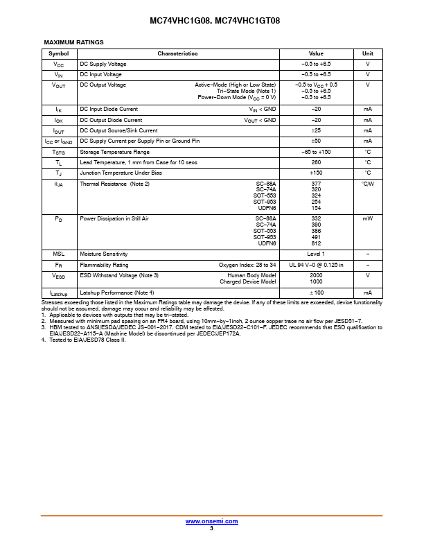
- Designed for 2.0 V to 5.5 V VCC Operation
- 3.5 ns tPD at 5 V (typ)
- Inputs/Outputs Over-Voltage Tolerant up to 5.5 V
- IOFF Supports Partial Power Down Protection
- Source/Sink 8 mA at 3.0 V
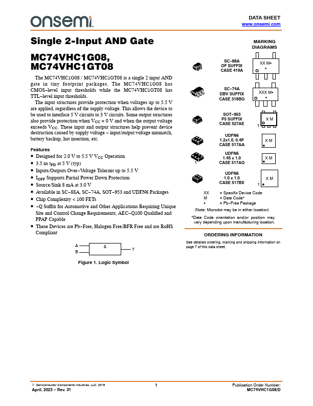
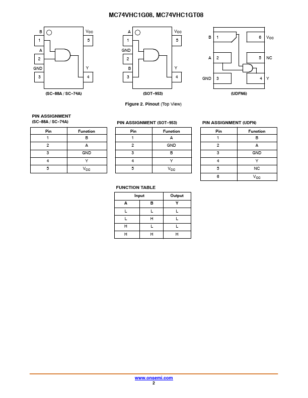
- Available in SC-88A, SC-74A, SOT-953 and UDFN6 Packages
- Chip plexity < 100 FETs
- Q Suffix for Automotive and Other