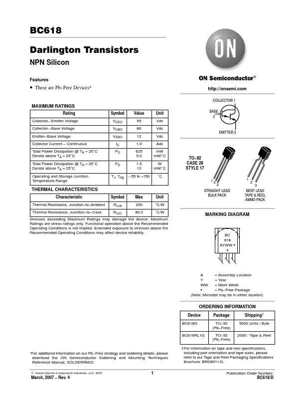
BC618 Overview
Key Features
- These are Pb-Free Devices*
| Part | BC618 |
|---|---|
| Description | Darlington Transistors |
| Category | Transistor |
| Manufacturer | onsemi |
| Size | 73.30 KB |
| Part Number | Manufacturer | Description |
|---|---|---|
| BC618 | NXP Semiconductors | NPN Darlington transistor |
| BC618 | Motorola Semiconductor | Darlington Transistors |
| BC618 | Siemens Semiconductor Group | NPN Silicon Darlington Transistors |
| BC618 | Philips Semiconductors | NPN Darlington transistor |
| BC6130 | CSR | Fully Qualified Single-chip Bluetooth-v2.1+EDR |