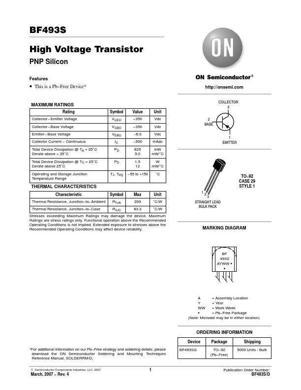
BF493S
BF493S is High Voltage Transistor manufactured by onsemi.
High Voltage Transistor
PNP Silicon
Features
- This is a Pb- Free Device-
MAXIMUM RATINGS Rating
Collector
- Emitter Voltage Collector
- Base Voltage Emitter
- Base Voltage Collector Current
- Continuous Total Device Dissipation @ TA = 25°C Derate above = 25°C
Symbol VCEO VCBO VEBO
IC PD
Value
- 350
- 350
- 6.0
- 500 625 5.0
Unit Vdc
Vdc Vdc mAdc mW mW/°C
Total Device Dissipation @ TC = 25°C Derate above 25°C
PD 1.5 W 12 mW/°C
Operating and Storage Junction Temperature Range
TJ, Tstg
- 55 to +150 °C
THERMAL CHARACTERISTICS
Characteristic
Symbol
Max
Unit
Thermal Resistance, Junction- to- Ambient...