CM1641
Description
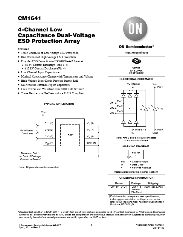
1 CH1 I/O LV Low−capacitance ESD Channel 2 CH2 I/O LV Low−capacitance ESD Channel 3 CH3 I/O LV Low−capacitance ESD Channel 4 VCC HV VDD HV ESD Channel 5 GND − Ground 6 7 8 DAP VN VN VN GND − Negative Voltage Supply Rail − Negative Voltage Supply Rail − Negative Voltage Supply Rail − Die Attach Pad (Ground) PACKAGE / PINOUT DIAGRAMS Top View (Pins Down View) 8765 Bottom View (Pins Up View) 1234 Pin 1 P41 Marking DAP 1234 8765 CM1641−04D4 8−Lead UDFN Package SPECIFICATIONS Table 2.
Key Features
- Three Channels of Low Voltage ESD Protection
- One Channel of High Voltage ESD Protection
- ±15 kV Contact Discharge (Pin 4)
- Low Channel Input Capacitance
- Minimal Capacitance Change with Temperature and Voltage
- High Voltage Zener Diode Protects Supply Rail
- No Need for External Bypass Capacitors
- Each I/O Pin can Withstand over 1000 ESD Strikes
- These Devices are Pb−Free and are RoHS pliant
Applications
- Die Attach Pad on Back of Package (Connect to Ground)