D44C12
Overview
- ăLow Collector-Emitter Saturation Voltage - 0.5 V (Max)
- ăHigh ft for Good Frequency Response
- ăLow Leakage Current
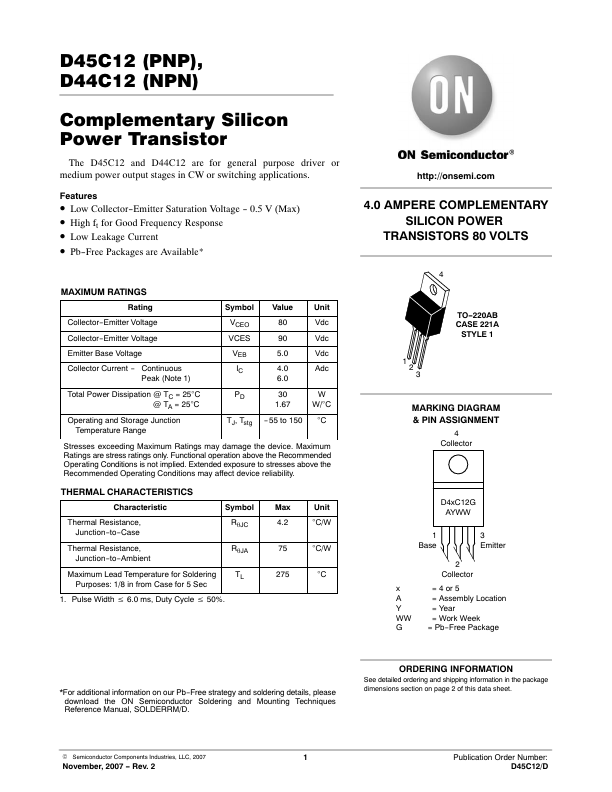
- ăPb-Free Packages are Available* ÎÎÎÎÎÎÎÎÎÎÎÎÎÎÎÎÎÎÎMAXIMUM RATINGS ÎÎÎÎÎÎÎÎÎÎÎÎÎÎÎÎÎÎÎRating Symbol Value Unit ÎÎÎÎÎÎÎÎÎÎÎÎÎÎÎÎÎÎÎCollector-Emitter Voltage ÎÎÎÎÎÎÎÎÎÎÎÎÎÎÎÎÎÎÎCollector-Emitter Voltage VCEO 80 Vdc VCES 90 Vdc ÎÎÎÎÎÎÎÎÎÎÎÎÎÎÎÎÎÎÎEmitter Base Voltage ÎÎÎÎÎÎÎÎÎÎÎÎÎÎÎÎÎÎÎCollector Current - Continuous Peak (Note 1) VEB 5.0 Vdc IC 4.0 Adc 6.0 ÎÎÎÎÎÎÎÎÎÎÎÎÎÎÎÎÎÎÎÎÎÎÎÎÎÎÎÎÎÎÎÎÎÎÎÎÎÎTotal Power Dissipation @ TC = 25°C Total Power Dissipation @ TA = 25°C ÎÎÎÎÎÎÎÎÎÎÎÎÎÎÎÎÎÎÎOperating and Storage Junction ÎÎÎÎÎÎÎÎÎÎÎÎÎÎÎÎÎÎÎTemperature Range PD TJ, Tstg 30 1.67 -ā55 to 150 W W/°C °C ÎÎÎÎÎÎÎÎÎÎÎÎÎÎÎÎÎÎÎStresses exceeding Maximum Ratings may damage the device. Maximum Ratings are stress ratings only. Functional operation above the Recommended ÎÎÎÎÎÎÎÎÎÎÎÎÎÎÎÎÎÎÎOperating Conditions is not implied. Extended exposure to stresses above the ÎÎÎÎÎÎÎÎÎÎÎÎÎÎÎÎÎÎÎRecommended Operating Conditions may affect device reliability. ÎÎÎÎÎÎÎÎÎÎÎÎÎÎÎÎÎÎÎTHERMAL CHARACTERISTICS ÎÎÎÎÎÎÎÎÎÎÎÎÎÎÎÎÎÎÎCharacteristic Symbol Max Unit ÎÎÎÎÎÎÎÎÎÎÎÎÎÎÎÎÎÎÎThermal Resistance, Junction-to-Case RqJC
- 2 °C/W ÎÎÎÎÎÎÎÎÎÎÎÎÎÎÎÎÎÎÎÎÎÎÎÎÎÎÎÎÎÎÎÎÎÎÎÎÎÎThermal Resistance, Junction-to-Ambient RqJA 75 °C/W ÎÎÎÎÎÎÎÎÎÎÎÎÎÎÎÎÎÎÎMaximum Lead Temperature for Soldering ÎÎÎÎÎÎÎÎÎÎÎÎÎÎÎÎÎ