D45C12 Overview
Key Specifications
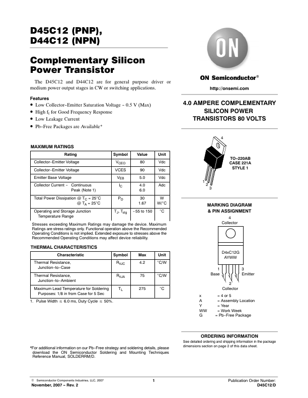
Package: TO-220AB
Mount Type: Through Hole
Pins: 3
Height: 6.35 mm
Key Features
- ăLow Collector-Emitter Saturation Voltage
- ăHigh ft for Good Frequency Response
- ăLow Leakage Current
- Continuous Peak (Note
| Part | D45C12 |
|---|---|
| Description | Complementary Silicon Power Transistor |
| Category | Transistor |
| Manufacturer | onsemi |
| Size | 69.36 KB |
Package: TO-220AB
Mount Type: Through Hole
Pins: 3
Height: 6.35 mm
| Seller | Inventory | Price Breaks | Buy |
|---|---|---|---|
| Verical | 1600 | 494+ : 0.7595 USD 549+ : 0.6835 USD 1000+ : 0.6304 USD 10000+ : 0.562 USD |
View Offer |
| Rochester Electronics | 1643 | 100+ : 0.6076 USD 500+ : 0.5468 USD 1000+ : 0.5043 USD 10000+ : 0.4496 USD |
View Offer |
| Part Number | Manufacturer | Description |
|---|---|---|
| D45C12 | Inchange Semiconductor | Silicon PNP Power Transistors |
| D45C12 | GE | PNP POWER TRANSISTORS |
| D45C12 | Mospec Semiconductor | Power Transistors |
| D45C10 | Inchange Semiconductor | Silicon PNP Power Transistors |
| D45C11 | Fairchild Semiconductor | PNP Current Driver Transistor |