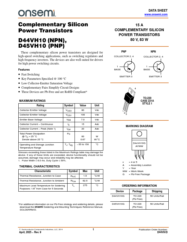
D45VH10
Features
- Fast Switching
- Key Parameters Specified @ 100 °C
- Low Collector-Emitter Saturation Voltage
- plementary Pairs Simplify Circuit Designs
- These Devices are Pb-Free and are Ro HS pliant-
MAXIMUM RATINGS
Rating
Symbol
Value
Unit
Collector-Emitter Voltage
Collector-Emitter Voltage
Emitter Base Voltage
Collector Current
- Continuous
Collector Current
- Peak (Note 1)
Total Power Dissipation @ TC = 25 °C Derate above 25 °C
VCEO VCEV VEB
IC ICM PD
80 100 7.0 15 20
83 0.67
Vdc Vdc Vdc Adc Adc
W W/°C
Operating and Storage Junction Temperature Range
TJ, Tstg
- 55 to 150
°C
Stresses exceeding those listed in the Maximum Ratings table may damage the device. If any of these limits are exceeded, device functionality should not be assumed, damage may occur and reliability may be affected. 1. Pulse Width ≤ 6.0 ms, Duty Cycle ≤ 50%.
THERMAL CHARACTERISTICS
Characteristic
Symbol Max
Thermal Resistance, Junction to Case
Rq JC
Thermal Resistance, Junction to Ambient
Rq...