EMT2DXV6T5 Overview
Key Specifications
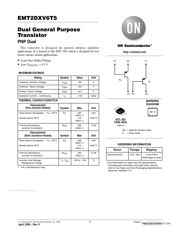
Package: SOT-563-6
Pins: 6
Max Operating Temp: 150 °C
Min Operating Temp: -55 °C
Key Features
- Lead-Free Solder Plating
- Low VCE(SAT), < 0.5 V
| Part | EMT2DXV6T5 |
|---|---|
| Description | Dual General Purpose Transistor |
| Category | Transistor |
| Manufacturer | onsemi |
| Size | 75.29 KB |
Package: SOT-563-6
Pins: 6
Max Operating Temp: 150 °C
Min Operating Temp: -55 °C
| Seller | Inventory | Price Breaks | Buy |
|---|---|---|---|
| Verical | 96000 | 6834+ : 0.0549 USD 10000+ : 0.0489 USD 100000+ : 0.041 USD |
View Offer |
| Rochester Electronics | 96000 | 100+ : 0.0529 USD 500+ : 0.0476 USD 1000+ : 0.0439 USD 10000+ : 0.0391 USD |
View Offer |
| Part Number | Manufacturer | Description |
|---|---|---|
| BDT88 | Inchange Semiconductor | Silicon PNP Power Transistor |
| KD333 | Tesla Elektronicke | Transistor |
| C828 | SEMTECH | NPN Silicon Transistor |