ESD11B Overview
Key Specifications
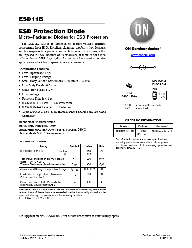
Pins: 2
Operating Voltage: 5 V
Length: 600 µm
Max Operating Temp: 125 °C
Key Features
- Low Capacitance 12 pF
- Low Clamping Voltage
- Small Body Outline Dimensions: 0.60 mm x 0.30 mm
- Low Body Height: 0.3 mm
- Stand-off Voltage: 5.0 V