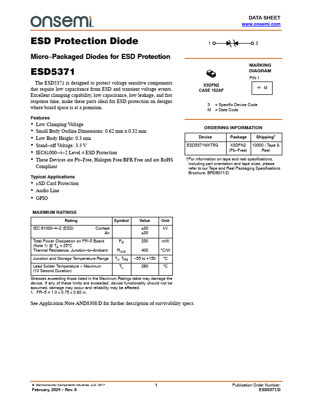
ESD5371 Overview
Semiconductor ponents Industries, LLC, 2017 1 February, 2024 − Rev. 6 Publication Order Number: ESD5371/D ESD5371 (TA = 25C unless otherwise noted) Symbol Parameter IPP Maximum Reverse Peak Pulse Current VC Clamping Voltage @ IPP VRWM Working Peak Reverse Voltage IR Maximum Reverse Leakage Current @ VRWM VBR Breakdown Voltage @ IT IT Test Current See Application Note AND8308/D for detailed explanations of...
ESD5371 Key Features
- Low Clamping Voltage
- Small Body Outline Dimensions: 0.62 mm x 0.32 mm
- Low Body Height: 0.3 mm
- Stand-off Voltage: 3.3 V
- IEC61000-4-2 Level 4 ESD Protection
- These Devices are Pb-Free, Halogen Free/BFR Free and are RoHS
ESD5371 Applications
- See Application Note AND8308/D for detailed explanations of datasheet parameters