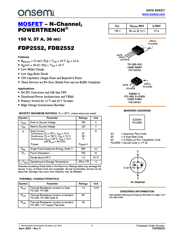
FDB2552
Features
- RDS(on) = 32 m W (Typ.), VGS = 10 V, ID = 16 A
- Qg(tot) = 39 n C (Typ.), VGS = 10 V
- Low Miller Charge
- Low QRR Body Diode
- UIS Capability (Single Pulse and Repetitive Pulse)
- These Devices are Pb- Free, Halide Free and are Ro HS pliant
Applications
- DC/DC Converters and Off- line UPS
- Distributed Power Architectures and VRMs
- Primary Switch for 24 V and 48 V Systems
- High Voltage Synchronous Rectifier
MOSFET MAXIMUM RATINGS (TC = 25°C, unless otherwise noted)
Symbol
Parameter
Ratings Unit
VDSS Drain to Source Voltage
VGS Gate to Source Voltage
±20
Drain Current
Continuous (TC = 25°C, VGS = 10 V)
Continuous (TC = 100°C, VGS = 10 V)
Continuous (Tamb = 25°C, VGS = 10 V,
5 with Rq JA = 43°C/W)
Pulsed
Figure 4
EAS Single Pulse Avalanche Energy (Note 1) PD Power Dissipation
Derate above 25°C
390 m J
W/°C
TJ, TSTG Operating and Storage Temperature
- 55 to 175 °C
Stresses exceeding those listed in the Maximum Ratings...