FDC6320C Overview
Description
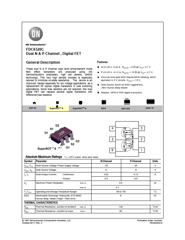
These dual N & P Channel logic level enhancement mode field effect transistors are produced using ON Semiconductor's proprietary, high cell density, DMOS technology. This very high density process is especially tailored to minimize on-state resistance.
Key Features
- N-Ch 25 V, 0.22 A, RDS(ON) = 5 Ω @ VGS= 2.7 V
- P-Ch 25 V, -0.12 A, RDS(ON) = 13 Ω @ VGS= -2.7 V
- Very low level gate drive requirements allowing direct operation in 3 V circuits
- Gate-Source Zener for ESD ruggedness
- >6kV Human Body Model Replace NPN & PNP digital transistors