FDC6331L
Description
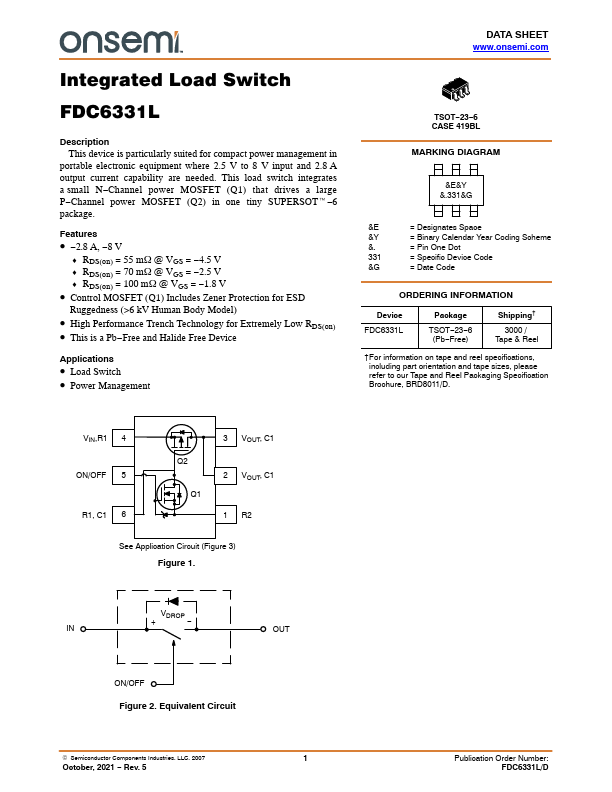
This device is particularly suited for pact power management in portable electronic equipment where 2.5 V to 8 V input and 2.8 A output current capability are needed.
Key Features
- RDS(on) = 55 mW @ VGS = −4.5 V
- RDS(on) = 70 mW @ VGS = −2.5 V
- RDS(on) = 100 mW @ VGS = −1.8 V
- Control MOSFET (Q1) Includes Zener Protection for ESD
- High Performance Trench Technology for Extremely Low RDS(on)
- This is a Pb−Free and Halide Free Device
Applications
- Load Switch