FDC6506P
Description
Features
These P-Channel logic level MOSFETs are produced using ON Semiconductor's advanced Power Trench process that has been especially tailored to minimize on-state resistance and yet maintain low gate charge for superior switching performance.
- -1.8 A, -30 V. RDS(on) = 0.170 Ω @ VGS = -10 V
RDS(on) = 0.280 Ω @ VGS = -4.5 V
- Low gate charge (2.3n C typical).
These devices have been designed to offer exceptional power dissipation in a very small footprint for applications where the bigger more expensive SO-8 and TSSOP-8 packages are impractical.
Applications
- Load switch
- Battery protection
- Power management
- Fast switching speed.
- High performance trench technology for extremely low RDS(ON).
- Super SOTTM-6 package: small footprint (72% smaller than standard SO-8); low profile (1mm thick).
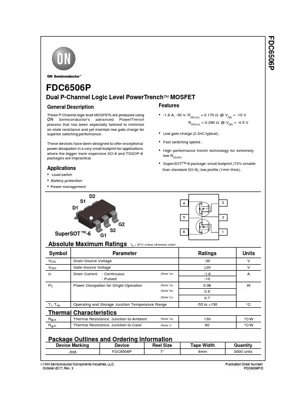
D2 S1
D1
G2
Super SOT TM -6
S2 G1
Absolute Maximum Ratings TA = 25°C unless otherwise noted
Symbol
Parameter
VDSS VGSS ID
Drain-Source Voltage...