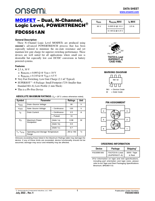
FDC6561AN
Description
These N- Channel Logic Level MOSFETs are produced using onsemi’s advanced POWERTRENCH process that has been especially tailored to minimize the on- state resistance and yet maintain low gate charge for superior switching performance. These devices are well suited for all applications where small size is desireable but especially low cost DC/DC conversion in battery powered systems.
Features
- 2.5 A, 30 V
- RDS(ON) = 0.095 W @ VGS = 10 V
- RDS(ON) = 0.145 W @ VGS = 4.5 V
- Very Fast Switching. Low Gate Charge (2.1 n C Typical)
- SUPERSOTt- 6 Package: Small Footprint (72% Smaller than
Standard SO- 8); Low Profile (1 mm Thick)
- This is a Pb- Free Device
ABSOLUTE MAXIMUM RATINGS (TA = 25°C unless otherwise noted)
Symbol
Parameter
Ratings Unit
VDSS Drain- Source Voltage
VGSS Gate- Source Voltage
- Continuous
±20
Drain Current
- Continuous
- Pulsed
Maximum Power
Dissipation
(Note 1a) (Note 1b)
(Note 1c)
TJ, TSTG Operating...