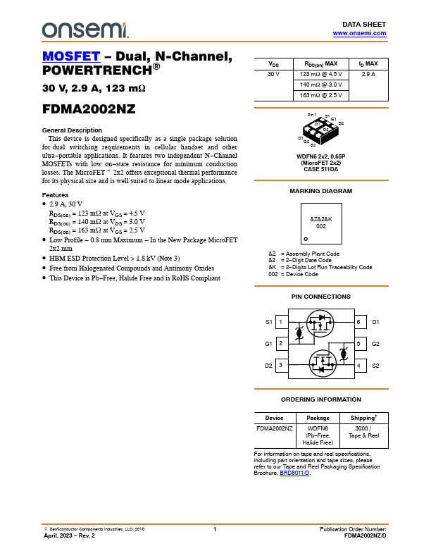
FDMA2002NZ
Description
This device is designed specifically as a single package solution for dual switching requirements in cellular handset and other ultra-portable applications. It features two independent N-Channel MOSFETs with low on-state resistance for minimum conduction losses.
Key Features
- 2.9 A, 30 V RDS(on) = 123 mW at VGS = 4.5 V RDS(on) = 140 mW at VGS = 3.0 V RDS(on) = 163 mW at VGS = 2.5 V
- 0.8 mm Maximum
- In the New Package MicroFET 2x2 mm
- HBM ESD Protection Level > 1.8 kV (Note
- Free from Halogenated pounds and Antimony Oxides