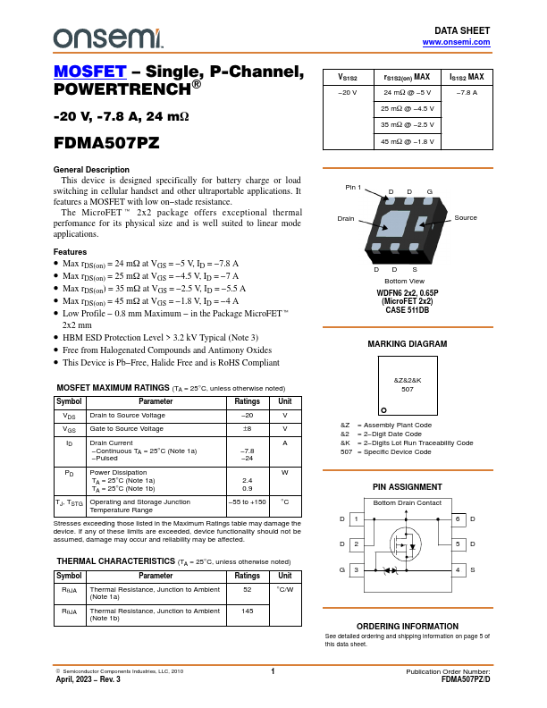
FDMA507PZ
Description
This device is designed specifically for battery charge or load switching in cellular handset and other ultraportable applications. It features a MOSFET with low on- stade resistance.
The Micro FET t 2x2 package offers exceptional thermal perfomance for its physical size and is well suited to linear mode applications.
Features
- Max r DS(on) = 24 m W at VGS =
- 5 V, ID =
- 7.8 A
- Max r DS(on) = 25 m W at VGS =
- 4.5 V, ID =
- 7 A
- Max r DS(on) = 35 m W at VGS =
- 2.5 V, ID =
- 5.5 A
- Max r DS(on) = 45 m W at VGS =
- 1.8 V, ID =
- 4 A
- Low Profile
- 0.8 mm Maximum
- in the Package Micro FETt
2x2 mm
- HBM ESD Protection Level > 3.2 k V Typical (Note 3)
- Free from Halogenated pounds and Antimony Oxides
- This Device is Pb- Free, Halide Free and is Ro HS pliant
MOSFET MAXIMUM RATINGS (TA = 25°C, unless otherwise noted)
Symbol
Parameter
Ratings Unit
VDS Drain to Source Voltage
VGS Gate to Source Voltage
ID Drain Current
- Continuous TA = 25°C (Note 1a)
- Pulsed
- 20
±8
- 7.8
-...