FDMA530PZ
Description
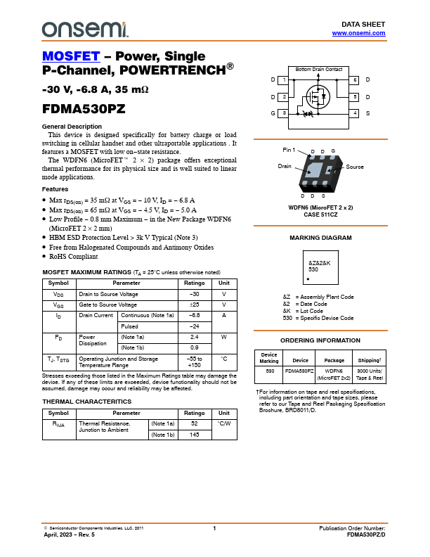
This device is designed specifically for battery charge or load switching in cellular handset and other ultraportable applications. It features a MOSFET with low on-state resistance.
Key Features
- Max rDS(on) = 35 mW at VGS =
- Max rDS(on) = 65 mW at VGS =
- 0.8 mm Maximum
- in the New Package WDFN6 (MicroFET 2 × 2 mm)
- HBM ESD Protection Level > 3k V Typical (Note
- Free from Halogenated pounds and Antimony Oxides
- RoHS compliant MOSFET Symbol Parameter Ratings Unit VDS Drain to Source Voltage
- 30 V VGS Gate to Source Voltage ±25 V ID Drain Current Continuous (Note 1a)
- 6.8 A Pulsed
- 24 PD Power (Note 1a) Dissipation (Note 1b) 2.4 W 0.9 TJ, TSTG Operating Junction and Storage Temperature Range