FDMD8430
Description
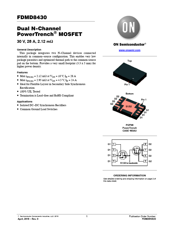
This package integrates two N- Channel devices connected internally in mon- source configuration. This enables very low package parasitics and optimized thermal path to the mon source pad on the bottom. Provides a very small footprint (3.3 x 5 mm) for higher power density.
Features
- Max r DS(on) = 2.12 m W at VGS = 10 V, ID = 28 A
- Max r DS(on) = 2.95 m W at VGS = 4.5 V, ID = 24 A
- Ideal for Flexible Layout in Secondary Side Synchronous
Rectification
- 100% UIL Tested
- Termination is Lead- free and Ro HS pliant
Applications
- Isolated DC- DC Synchronous Rectifiers
- mon Ground Load Switches
.onsemi. Top
Pin 1
D2 D2
D2
G2
Bottom S1/S2
Pin 1
G1 D1 D1 D1
PQFN8 Power Trench CASE 483AU
G1 1 D1 2 D1 3 D1 4
S1,S2 to backside
8 D2 7 D2 6 D2 5 G2
ORDERING INFORMATION
See detailed ordering and shipping information on page 2 of this data sheet.
© Semiconductor ponents Industries, LLC, 2018
April, 2018
- Rev. 0
Publication Order Number: FDMD8430/D
Table 1. MOSFET...