FDMS1D2N03DSD
Description
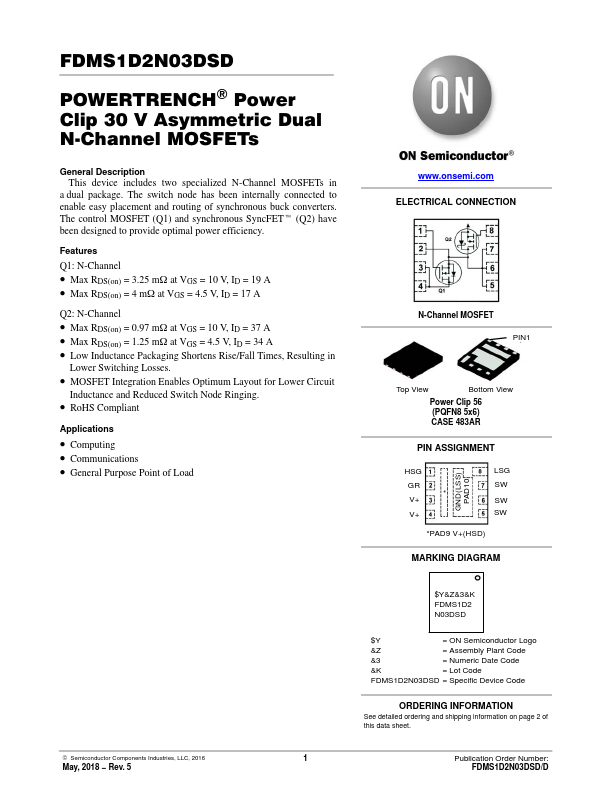
This device includes two specialized N-Channel MOSFETs in a dual package. The switch node has been internally connected to enable easy placement and routing of synchronous buck converters. The control MOSFET (Q1) and synchronous Sync FETt (Q2) have been designed to provide optimal power efficiency.
Features
Q1: N-Channel
- Max RDS(on) = 3.25 m W at VGS = 10 V, ID = 19 A
- Max RDS(on) = 4 m W at VGS = 4.5 V, ID = 17 A
Q2: N-Channel
- Max RDS(on) = 0.97 m W at VGS = 10 V, ID = 37 A
- Max RDS(on) = 1.25 m W at VGS = 4.5 V, ID = 34 A
- Low Inductance Packaging Shortens Rise/Fall Times, Resulting in
Lower Switching Losses.
- MOSFET Integration Enables Optimum Layout for Lower Circuit
Inductance and Reduced Switch Node Ringing.
- Ro HS pliant
Applications
- puting
- munications
- General Purpose Point of Load
.onsemi. ELECTRICAL CONNECTION
N-Channel MOSFET
PIN1
Top View
Bottom View
Power Clip 56 (PQFN8 5x6) CASE 483AR
PIN ASSIGNMENT
HSG GR V+ V+
- GND(LSS)
PAD10
LSG SW SW...