Datasheet4U.com
🌙
FJV42 Datasheet | onsemi
Part:
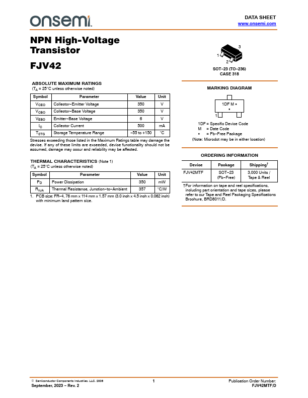
FJV42
Description:
NPN High-Voltage Transistor
Category:
Transistor
Manufacturer:
onsemi
Size:
151.76 KB
Download FJV42 Datasheet PDF
onsemi
FJV42
FJV42 is NPN High-Voltage Transistor manufactured by onsemi.
FJV42 Datasheets by Manufacturer
Manufacturer
Part Number
Description
Fairchild Semiconductor
FJV42
NPN High Voltage Transistor
×
Close