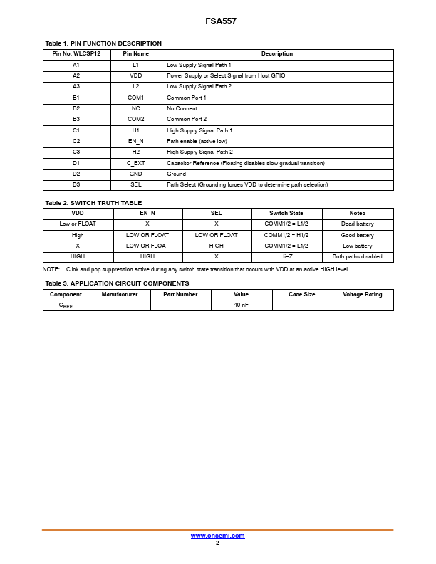
Datasheet4U Logo Datasheet4U.com

FSA557 - Low Supply Signal Bypass-IC

General Description

Pin No.

Key Features

  • Dual Depletion Switches.
  • Normally Closed when VDD < 0.5 V.
  • VSW:.
  • 1.5 V to +5.5 V.
  • RON: 220 mW (Typical).
  • THD+N:.
  • 110 dB (Typical).
  • Dual Enhancement Switches.
  • VSW:.
  • 1.5 V to +5.5 V.
  • RON: 290 mW (Typical).
  • THD+N:.
  • 113 dB (Typical) Typical.

📥 Download Datasheet

Datasheet Details

Part number FSA557
Manufacturer onsemi
File Size 203.99 KB
Description Low Supply Signal Bypass-IC
Datasheet download datasheet FSA557 Datasheet

Full PDF Text Transcription (Reference)

The following content is an automatically extracted verbatim text from the original manufacturer datasheet and is provided for reference purposes only.

View original datasheet text
Low Supply Signal Bypass IC Product Preview FSA557 The FSA557 integrates 0.3 W depletion and enhancement mode switches to provide a signal bypass solution when batteries of wireless devices are low or have no charge left. In addition, an optional slow gradual transition is included to suppress any undesirable artifacts (ex: click and pop) when switching between signal sources. The depletion technology allows the device to conduct signals when there is no VDD available and to isolate signals when VDD is present. The FSA557 is 5.5 V tolerant and can pass or isolate negative signal swings down to −1.5 V. Features • Dual Depletion Switches ♦ Normally Closed when VDD < 0.5 V ♦ VSW: −1.5 V to +5.5 V ♦ RON: 220 mW (Typical) ♦ THD+N: −110 dB (Typical) • Dual Enhancement Switches ♦ VSW: −1.