HC240A
Features
- Output Drive Capability: 15 LSTTL Loads
- Outputs Directly Interface to CMOS, NMOS, and TTL
- Operating Voltage Range: 2.0 to 6.0 V
- Low Input Current: 1 m A
- High Noise Immunity Characteristic of CMOS Devices
- In pliance with the Requirements Defined by JEDEC Standard
No. 7 A
- Chip plexity: 120 FETs or 30 Equivalent Gates
- NLV Prefix for Automotive and Other Applications Requiring
Unique Site and Control Change Requirements; AEC- Q100 Qualified and PPAP Capable
- These Devices are Pb- Free, Halogen Free and are Ro HS pliant
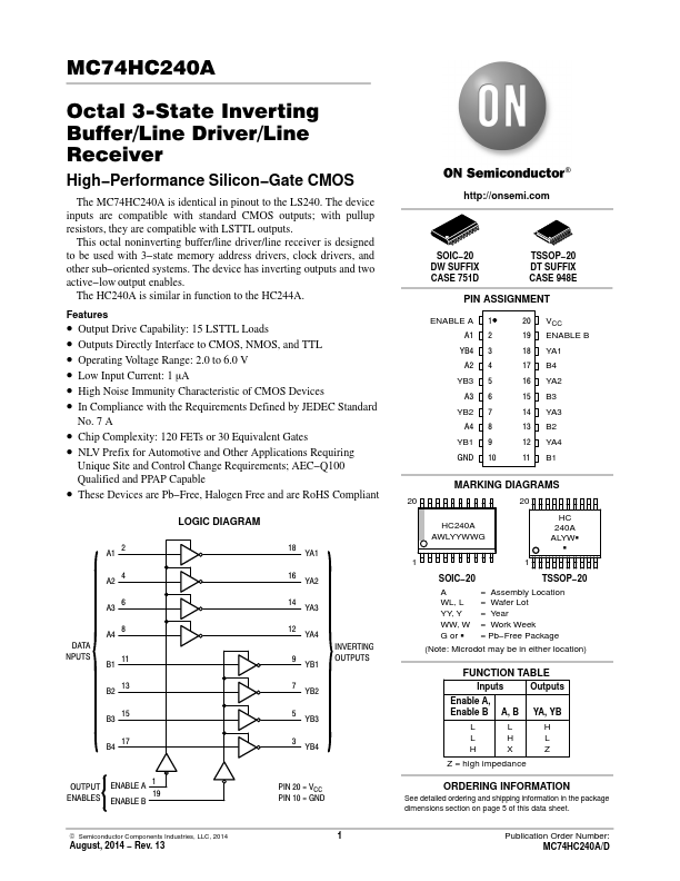
LOGIC DIAGRAM
A1 2
A2 4
A3 6
DATA NPUTS
A4 8 B1 11
B2 13
B3 15
B4 17
18 YA1
16 YA2
14 YA3
12 YA4 9 YB1
INVERTING OUTPUTS
7 YB2
5 YB3
3 YB4
OUTPUT ENABLE A 1
ENABLES
19 ENABLE B
PIN 20 = VCC PIN 10 = GND
© Semiconductor ponents Industries, LLC, 2014
August, 2014
- Rev. 13 http://onsemi.
SOIC- 20 DW SUFFIX CASE 751D
TSSOP- 20 DT SUFFIX CASE 948E
PIN...