HGT1S7N60A4DS
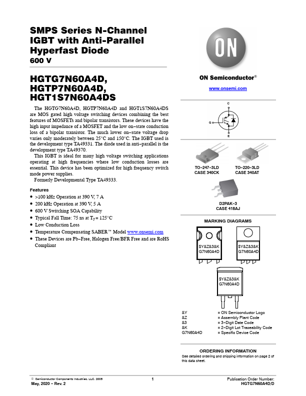
Description
Symbol All Types Units Collector to Emitter Voltage Collector Current Continuous At TC = 25°C At TC = 110°C BVCES 600 V IC25 34 A IC110 14 A Collector Current Pulsed (Note 1) Gate to Emitter Voltage Continuous Gate to Emitter Voltage Pulsed Switching Safe Operating Area at TJ = 150°C (Figure 1) Power Dissipation Total at TC = 25°C Power Dissipation Derating TC > 25°C ICM VGES VGEM SSOA PD 56 ±20 ±30 35 A at 600 V 125 1.0 A V V W W/°C Operating and Storage Junction Temperature Range TJ, TSTG −55 to 150 °C Maximum Lead Temperature for Soldering Leads at 0.063 in (1.6 mm) from case for 10 s Package Body for 10 s, see Tech Brief 334 TL 300 TPKG 260 Stresses exceeding those listed in the .onsemi.
Key Features
- >100 kHz Operation at 390 V, 7 A
- 200 kHz Operation at 390 V, 5 A
- 600 V Switching SOA Capability
- Typical Fall Time: 75 ns at TJ = 125°C
- Low Conduction Loss