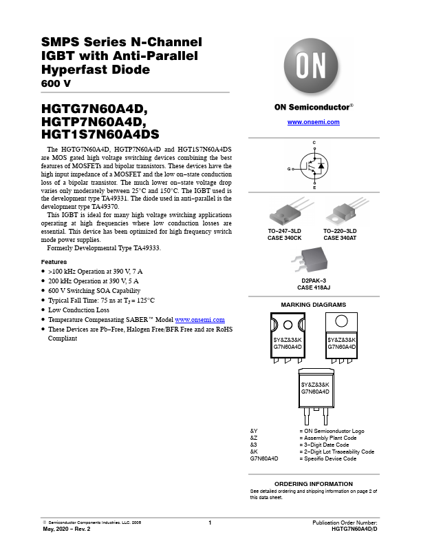
Description
Symbol All Types Units Collector to Emitter Voltage Collector Current Continuous At TC = 25°C At TC = 110°C BVCES 600 V IC25 34 A IC110 14 A Collector Current Pulsed (Note 1) Gate to Emitter Voltage Continuous Gate to Emitter Voltage Pulsed Switching Safe Operating Area at TJ = 150°C (Figure 1) Power Dissipation Total at TC = 25°C Power Dissipation Derating TC > 25°C ICM VGES VGEM SSOA PD 56 ±20 ±30 35 A at 600 V 125 1.0 A V V W W/°C Operating and Storage Junction Temperature Range TJ, TSTG -55 to 150 °C Maximum Lead Temperature for Soldering Leads at 0.063 in (1.6 mm) from case for 10 s Package Body for 10 s, see Tech Brief 334 TL 300 TPKG 260 Stresses exceeding those listed in the .onsemi. 2 HGTG7N60A4D, HGTP7N60A4D, ELECTRICAL SPECIFICATIONS TJ = 25 °C Unless Otherwise Specified PARAMETER SYMBOL TEST CONDITIONS MIN TYP MAX UNITS Collector to Emitter Breakdown Voltage Collector to Emitter Leakage Current BVCES ICES IC = 250 mA, VGE = 0 V VCE = 600 V TC = 25°C 600 - - V - - 250 mA TC = 125°C - - 2 mA Collector to Emitter Saturation Voltage VCE(SAT) IC = 7 A, VGE = 15 V TC = 25°C TC = 150°C - 1.9 2.7 V - 1.6 2.2 V Gate to Emitter Threshold Voltage Gate to Emitter Leakage Current Switching SOA VGE(TH) IGES SSOA IC = 250 mA, VCE = 600 V VGE = ±20 V TJ = 150°C, RG = 25 Ω, VGE = 15 V, L = 100 mH, VCE = 600 V 4.5 5.9 7 V - - ±250 nA 35 - - A Gate to Emitter Plateau Voltage VGEP IC = 7 A, VCE = 300 V - 9 - V On-State Gate Charge Current Turn-On Delay Time Current Rise Time Current Turn-Off Delay Time Current Fall Time Turn-On Energy Turn-On Energy QG(ON) td(ON)I trI td(OFF)I tfI EON1 EON2 IC = 7 A, VC.
Key Features
- >100 kHz Operation at 390 V, 7 A
- 200 kHz Operation at 390 V, 5 A
- 600 V Switching SOA Capability
- Typical Fall Time: 75 ns at TJ = 125°C
- Low Conduction Loss
- Temperature pensating SABER™ Model .onsemi