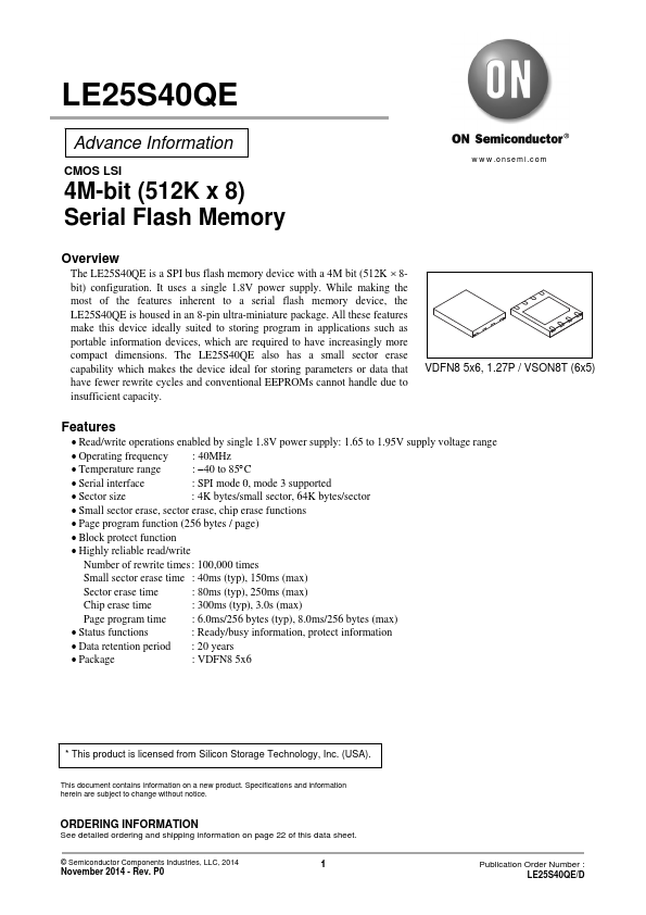
LE25S40QE Overview
Key Specifications
Operating Voltage: 1.8 V
Max Voltage (typical range): 1.95 V
Min Voltage (typical range): 1.65 V
Max Frequency: 40 MHz
Key Features
- Read/write operations enabled by single 1.8V power supply: 1.65 to 1.95V supply voltage range
- Operating frequency : 40MHz
- Temperature range : -40 to 85°C
- Serial interface : SPI mode 0, mode 3 supported
- Sector size : 4K bytes/small sector, 64K bytes/sector